
uniLDD 概要
EKSPLA社製は、長年に渡りレーザー及びレーザーに関する電気機器の製造・販売を行っており、常に最先端の製品を世に送り出しています。
特にハイパワーエレクトロニクス(高速/高電圧電源)は、EKSPLAが得意とするコア技術の一つです。
R&DからOEMまでと幅広い用途に対応するために、お客様のご要望に応じたカスタマイズも承っておりますので、お気軽にお問い合わせください。
Features
| 半導体レーザー用ドライバ(Universal Laser Diode Driver) クリックするとメーカーホームページに移動します。 |
|
|---|---|
 |
uniLDD is DC input power converter designed to supply |
|
|
Analog Control Signals
Description of Analog interface pinout
Connector type: 15 pin D-SUB female
| Pin | Signal name | Direction | Voltage level | Description |
|---|---|---|---|---|
| 1 | Enable | Input | TTL, LVTTL | The enable function pulls the RTO signal high |
| 2 | Ready to Operate (RTO) | Input/Output through 330 Ω resistor |
>2.4 V driver output is active, <0.5 V output is clamped |
RTO is tied to "High" by the driver when "Enable" input is High. Alarms clamp RTO low and disable driver output. External device may clamp RTO to GND and disable driver output. RTO allows to join fault circuits of several drivers connected in parallel |
| 3 | Interlock | Input | 10 kΩ pull up to 3.3 V, LOW ≤ 0.4 V |
The Interlock function can be connected to external safety or machine protection switches such as door or temperature switches. Open = OFF Connect to GND = RUN |
| 4 | GND | – | – | – |
| 5 | Vout monitor | Output | Vout, driver output voltage | The output voltage monitor. Vout = Diode compliance voltage + voltage drop on connection wires |
| 6 | Iout monitor | Output | 0 – 12 V 1) = 0 – Iout max | The output current monitor |
| 7 | Iprogram | Input | 0 – 9 V 1) = 0 – Iout max | Output current setting or modulating by applying a voltage, CW and Pulse mode |
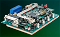
Performance & Drawings
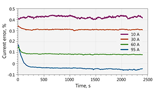
uniLDD current drift.
From cold start for
different currents
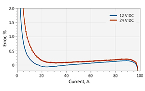
uniLDD current error.
12 V and 24 V DC power,
2 V junction + 10 MΩ series
R load
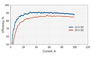
uniLDD efficiency.
12 V and 24 V DC power,
2 V junction + 10 MΩ series R
load
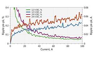
uniLDD current error.
12 V and 24 V DC power,
2 V junction + 10 MΩ series R
load
CW version.
Capacitors bank is excluded
CW version.
Capacitors bank is excluded
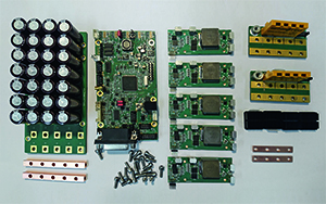
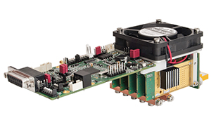
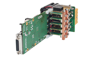
Modular design.
Required features and
specifications are achieved by combining
different boards to one module
仕様
| Parameter | Value 1) 2) | Notes |
|---|---|---|
| OUTPUT, CW mode | ||
| Diode compliance voltage | 1 … 28 V | Up to 95% of power stage supply voltage. Can be extended using voltage booster layout |
| Max current | 50 – 100 A | Can be extended above 100 A using parallel connection of several drivers |
| Current ripple | 0.1% pk-pk | DC … 100 kHz bandwidth, in x0.5 … x1 of max current range |
| Current drift | < 0.2% | Cold start, 8 h period, after 5 min. warm up |
| Bandwidth of Iprogramm control input frequency | > 10 kHz | At minimal connection cable inductance |
| OUTPUT, OCW (Pulse mode) | ||
| Diode compliance voltage | 1 … 80 V | Can be extended using voltage booster layout |
| Max pulse current | 160 – 360 A | Can be extended above 360A using parallel connection of the drivers |
| Duty cycle | ≤ 20% | |
| Current pulse raise, typical range | 10 … 50 μs | @ minimal connection cable inductance and sufficient power stage voltage |
| Max RMS current | 100 A | 80 A for diode compliance voltage gt; 28 V |
| Current pulse amplitude stability | 0.1% pk-pk | In x0.5…x1 of max current range |
| Current drift | < 0.2% | Cold start, 8 h period, after 5 min. warm up |
| OUTPUT, TEC control (if equipped) | ||
| Quantity of output channels | 1 or 2 | |
| Maximal output current | 25 A | |
| Maximal output voltage | 28 V | |
| INPUT | ||
| Supply voltage, power stage | 12… 90 VDC | |
| Supply voltage, control stage | 12 … 30 VDC | |
| PROTECTIONS | ||
| Current transient protection | Shut-down | |
| Open circuit | Shut-down | |
| Over temperature | Shut-down | |
| Power voltage brownout | Shut-down | |
| Interlock | Shut-down | |
| AUXILIARY OUTPUTS | ||
| Aux1 | +5 V @ 200 mA | |
| Aux2 | +15 V @ 100 mA | |
| Aux3 | -15 V @ 100 mA | |
| PHYSICAL CHARACTERISTICS | ||
| Assembly dimensions (L×W×H) | 190×68×55 mm | |
| ENVIRONMENT | ||
| Operating temperature | 0 to 40°C | De-rate current at higher temperature |
| Cooling | Forced air | Installed or external shared fan. Conductive cooling version available as option |
- 1. Specifications are subject to change without prior notice.
- 2. Not all combinations of parameters are possible at the same time.
ダウンロードしたPDFファイルをご覧になるには、Adobe Acrobat Readerが必要です。左記のバナーより、ソフトウェア(無料)をダウンロード・インストールして下さい。
| 更新日 | 更新内容 | サイズ | ダウンロード |
|---|